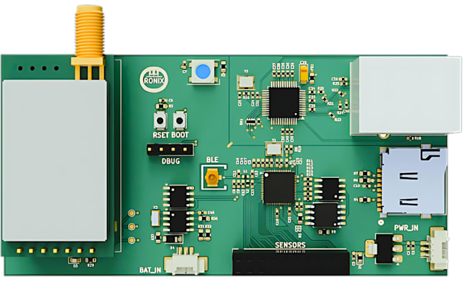
Se stai creando un dispositivo IoT, un sensore embedded o un gateway industriale e hai bisogno di un progetto PCB solido, sono un ingegnere di sistemi embedded con oltre 5 anni di esperienza pratica in hardware ESP32, LoRa, Modbus e Wi-Fi. Dalla cattura dello schema iniziale alla produzione di Gerber pronte.
Ciò che include
- Schema chiaro e annotato
- Layout PCB ottimizzato con distanze e posizionamento componenti corretti
- File Gerber e drill pronti per la produzione
- Modello 3D per integrazione nell' enclosure
- (Livello complesso) Strategia di integrità del segnale e dell'alimentazione
Scegli il tuo pacchetto:
- Pacchetto PCB semplice (2 strati) Prototipi rapidi fino a 30 componenti
- Pacchetto PCB intermedio (4 strati, bassa velocità) Schede multi-layer standard
- Progettazione PCB complessa Progetti ad alta velocità/misto-sigla con impedenza controllata, coppie differenziali e stacking avanzato di piani di alimentazione