Sfoglia categorie
Italiano
$
USD
Connettiti alla tua IA
edwardpcb
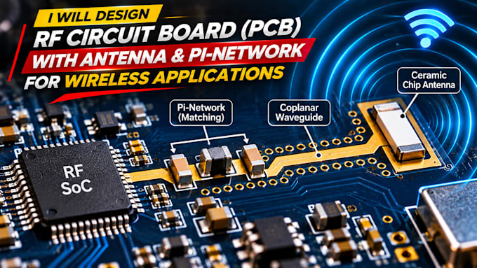
Is your custom IoT device suffering from poor Bluetooth connection range, dropped WiFi packets, or failing regulatory emissions testing? At high frequencies, a standard PCB trace behaves like a complex transmission line. Simple layout oversight can completely ruin your wireless signal integrity.
I provide expert RF PCB layout engineering, antenna impedance matching, and wireless circuit optimization designed to maximize range and achieve reliable field operation.
Instead of dealing with unpredictable signal loss, I calculate precise copper geometries and construct matching pi-networks to deliver flawless 50-ohm transmission lines straight to your antenna.
RF Problems I Solve:
What You Receive:
Specializzazione:
Progettazione circuito
•
Schematics
•
Gerber
Formato di file:
Gerber
•
Software:
Allegro
•
Altium Designer
•
Eagle CAD
•
EasyEDA
•
KiCad
