Sfoglia categorie
Esplora
Fiverr Pro
Italiano
$
USD

Level 2
Sr Electronics Product Design Expert , Altium PCB Circuit Hardware Gerbers
Competenze
Consulta i miei servizi
Vuoi lavorare su base oraria?
Spiega a Avi Gupta cosa ti serve.
30 USD
/
ora
Sr. Technical Hardware Specialist
Philips India • Full time
May 2017 - Mar 2019 • 1 yr 10 mos
At Philips Lighting, I was entrusted with a crucial role in the hardware design and development of smart LED and IoT-based products, contributing to the advancement of connected lighting solutions. Working alongside a dynamic team, I led the development of hardware from initial concept to fully tested prototypes, which were successfully brought to mass production. Key Responsibilities: 1. Hardware Development: Led the hardware design for solar-powered LED drivers and connectivity-based products, transforming requirements into fully functional, certified prototypes. 2. Schematic & PCB Design: Utilized Altium and Mentor Graphics to capture schematics and design PCBs for cutting-edge smart lighting products. 3. Supplier Coordination: Collaborated with suppliers to arrange component samples and ensure adequate inventory, while managing relationships for timely procurement. 4. Component Risk Management: Mitigated supply chain risks by identifying alternate vendors and securing a steady supply of critical components. 5. Testing & Certification: Conducted thorough testing and validation, ensuring products met stringent industry certifications such as EMI/EMC, CE, and UL. 6. LED Module Optimization: Optimized LED module performance, specifically focusing on improving lumen efficacy to enhance product efficiency. Achievements: 1. Successfully transitioned products from concept to mass production, playing a vital role in Philips' innovative smart lighting solutions. 2. Enhanced product performance through strategic design optimizations and rigorous testing, contributing to improved market competitiveness.

Hardware Engineer
TOSHIBA • Full time
Mar 2013 - Apr 2017 • 4 yrs 1 mo
Worked as a Hardware Design Engineer on electronic products from circuit concept and schematic design through PCB development, validation, EMI/EMC improvement and production support. Key responsibilities: • Designed and optimized SMPS, buck converters, capacitive power supplies, protection circuits and power-distribution sections for embedded products. • Developed and reviewed analog, digital and mixed-signal circuits involving ADCs, EEPROMs, ASICs, microcontrollers, sensors and communication interfaces. • Created and optimized PCB layouts for grounding, return paths, signal integrity, thermal performance, manufacturability and EMI/EMC compliance. • Performed schematic review, PCB design review, component selection, derating analysis, DFMEA, MTBF estimation, DFR, DFM and production-readiness checks. • Conducted validation and troubleshooting for conducted emissions, radiated emissions, EFT, surge, impulse, high voltage and immunity-related failures. • Used oscilloscopes, spectrum analyzers, programmable power supplies, multimeters, GTEM cells, anechoic chambers and EMI/EMC test equipment. • Supported prototype bring-up, root-cause analysis, corrective redesign, calibration, design verification and transition to mass production. • Used Altium Designer, OrCAD, PSpice and MATLAB for schematic capture, PCB design, simulation and engineering analysis. Achievements: • Improved product reliability, EMC performance and manufacturing readiness through structured design optimization and verification. • Reduced component, PCB and production costs through practical circuit and process improvements. • Helped move products from prototype validation to stable mass production with clear documentation and production support. Core expertise: PCB design, PCB layout, schematic design, circuit design, hardware design, power electronics, embedded systems, analog design, mixed-signal design, EMI/EMC, DFM, DFR, DFMEA, troubleshooting and product validation.
| (21) | ||
| (0) | ||
| (0) | ||
| (1) | ||
| (0) |
coolad

Regno Unito
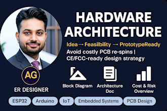
Thorough architecture work. Clear reasoning behind every decision, honest about what was uncertain rather than glossing over it, and flagged several issues early that would have been expensive to find later. Good documentation and responsive throughout.
Risposta del venditore

taylerburbury

Stati Uniti
tom_vallis
Regno Unito
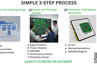
Fantastic work. Delivered a very detailed report that highlighted EMC/EMI design issues with the PCB and schematic design, listing all the changes required to ensure compliance with the relevant standards. Would definitely work with Avi more in the future.
Risposta del venditore
marco_gruber_kw

Svizzera
Great experience working with Avi. He’s professional, communicative, and clearly puts thought into every stage of the design process. Looking forward to continuing the collaboration!
marco_gruber_kw
Svizzera
Avi is a highly professional and detail-oriented engineer. He takes the time to deeply understand the technical requirements and communicates clearly throughout the process. His work on our project has been precise, thoughtful, and aligned with best practices. Highly recommended!