Sfoglia categorie
Esplora
Fiverr Pro
Italiano
$
USD
Esperto in progettazione PCB
Progettare un PCB ad alta velocità richiede più che collegare tracce. Serve un routing accurato, impedenza controllata, integrità del segnale e competenze di produzione.
Offro servizi avanzati di progettazione di PCB multilayer ad alta velocità per ingegneri, startup e aziende che sviluppano prodotti elettronici affidabili.
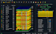
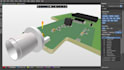
Questo servizio include revisione dello schema, layout di PCB multilayer, routing con impedenza controllata, progettazione RF PCB, routing di coppie differenziali, matching delle lunghezze, file Gerber, BOM, file Pick and Place, revisione DFM e documentazione pronta per la produzione.
Progetto schede ottimizzate per applicazioni ad alta frequenza e alta velocità, minimizzando EMI, perdita di segnale, crosstalk e rumore.
Utilizzo Altium Designer, KiCad e EasyEDA per sviluppare layout di PCB pronti alla produzione per sistemi di comunicazione, dispositivi embedded, elettronica industriale, applicazioni RF, hardware di rete e circuiti digitali.
Ogni progetto segue le migliori pratiche del settore per migliorare le prestazioni, semplificare l'assemblaggio e ridurre i rischi di produzione.
Che tu stia iniziando un nuovo progetto o migliorando un PCB esistente, consegno layout precisi, comunicazione chiara e consegna puntuale.
CONTATTAMI ORA. Iniziamo subito.
Traduzione automatica.
Di cosa hai bisogno prima di iniziare il mio PCB?
Fornisci lo schema, i requisiti di progettazione, le dimensioni della scheda, i dettagli dello stack-up, i requisiti di interfaccia o eventuali file di riferimento disponibili.
Puoi progettare PCB con impedenza controllata?
Sì. Progetto PCB con impedenza controllata, calcolo della larghezza delle tracce, routing di coppie differenziali e considerazioni sullo stack-up per prestazioni affidabili del segnale.
Progetti PCB RF e ad alta frequenza?
Sì. Progetto PCB RF per comunicazioni wireless, antenne, circuiti ad alta frequenza e altre applicazioni che richiedono routing accurato e integrità del segnale.
Puoi fare routing di interfacce DDR, USB, Ethernet o PCIe?
Sì. Posso fare routing di interfacce ad alta velocità come memoria DDR, USB, HDMI, Ethernet, PCIe, LVDS, SPI, I2C e altri bus di comunicazione ad alta velocità.
Quali file riceverò dopo la consegna?
Riceverai file Gerber, layout PCB, BOM, file Pick and Place, disegni di produzione e altra documentazione pronta per la fabbricazione in base al pacchetto scelto.
La PCB sarà pronta per la produzione?
Assolutamente. Ogni progetto viene sottoposto a revisione DFM ed è consegnato con file pronti per la produzione compatibili con produttori di PCB professionali.
Devo inviarti un messaggio prima di ordinare?
Sì. Contattarmi prima ci permette di rivedere i tuoi requisiti, scegliere il pacchetto giusto e assicurare che il tuo PCB sia progettato per soddisfare i tuoi obiettivi tecnici e di produzione.


