Sfoglia categorie
Esplora
Fiverr Pro
Italiano
$
USD

Skilled PCB design, schematic design, pcb layout, altium designer
Competenze
Consulta i miei servizi
.png)
Fiverr
Freelance • 11 yrs 9 mos
PCB Design & Electronics Engineer
Oct 2022 - Present • 3 yrs 11 mos
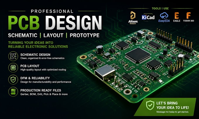
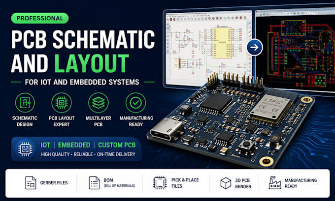
Provided PCB design and electronics engineering services for custom hardware and product development projects. Worked on circuit design, schematic capture, PCB layout, component placement, routing, Gerber preparation, BOM development, DFM review, and prototype preparation. Projects included embedded systems, Arduino, ESP32, IoT, motor drivers, power electronics, RF applications, and custom electronic products. Focused on practical, manufacturable, and production ready PCB solutions.
Embedded Systems & Electronics Engineer
Oct 2022 - Present • 3 yrs 11 mos
Worked on embedded electronics projects involving microcontrollers, Arduino, ESP32, IoT devices, sensors, motor control, and custom electronic systems. Developed and reviewed circuit schematics, selected components, created PCB layouts, and supported prototype development. Key achievements include designing reliable electronic circuits, integrating sensors and microcontrollers, optimizing component placement and PCB routing, and preparing designs for prototyping and manufacturing. Experienced in troubleshooting circuit issues, improving PCB performance, and translating project concepts into practical electronic solutions.
PCB Layout & Manufacturing Design Specialist
Oct 2022 - Present • 3 yrs 11 mos
Specialized in professional PCB layout, PCB design optimization, and design for manufacturing (DFM). Worked with 2-layer and multilayer PCB designs, SMT and THT components, component placement, routing, ground planes, power distribution, clearances, vias, and manufacturing requirements. Key achievements include preparing production-ready PCB files, validating Gerber and drill files, creating BOM and Pick and Place documentation, reviewing PCB layouts for manufacturing issues, and improving designs for reliability and cost-effective production. Experienced with Altium Designer, KiCad, EasyEDA, Eagle PCB, and Fusion 360.
