h
homagepcb

Abolade

@homagepcb
5,0(1)

pcb routing, multilayer pcb, BGA routing, HDI pcb, gerber files

Nigeria
Inglese
Alcune informazioni sono riportate in lingua inglese.
Chi sono
I’m a PCB design engineer specializing in HDI PCB layout, BGA routing, multilayer PCB design, and high-density circuit board layouts. I help startups, electronics engineers, and hardware developers turn schematics and existing PCB designs into clean, reliable, manufacturing-ready boards. For complex HDI, BGA, high-speed, or multilayer projects, send me your schematic, PCB files, layer requirements, board dimensions, and component information so I can review the scope before you order. thanks for reaching out, peace!... Continua a leggere

Competenze

h
homagepcb
Abolade
offline • 
Tempo di risposta medio: 1 ora

Consulta i miei servizi

Circuito stampato (PCB)
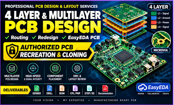
I will design 4 layer multilayer pcb, easyeda pcb, redesign with gerber files
5,0(1)
Circuito stampato (PCB)
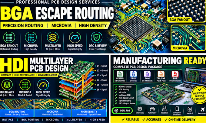
I will design high speed hdi pcb, multilayer pcb with bga and microvia routing

1 Recensioni
5,0

(1)
(0)
(0)
(0)
(0)
Valutazione dettagliata
  • Livello di comunicazione del venditore
    5
  • Qualità della consegna
    5
  • Valore della consegna
    5
1-1 di 1 recensioni
Ordina per
Più rilevante
    O

    ouzouniszisis19

    GR

    Grecia

    5

    Abolande is an exceptional engineer! He has a deep understanding of hardware design and an incredible attention to detail. He completely audited our 4-layer PCB layout, caught critical mistakes from previous designs, and re-routed the high-power section for our TO-220 MOSFETs perfectly with 0 DRC errors....

    50 USD-100 USD

    $

    4 settimane

    Tempo

    gig

    Circuito stampato (PCB)

    Utile?
    Sì
    No