Alcune informazioni sono riportate in lingua inglese.
Chi sono
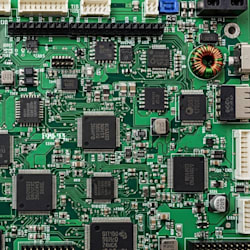
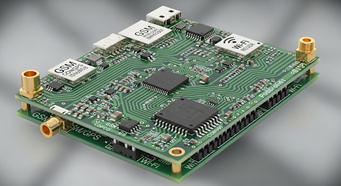
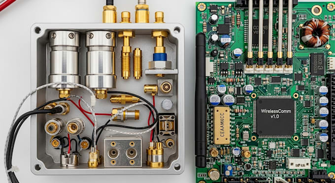
I am a professional PCB Layout Designer and Electronics Hardware Developer with strong experience in transforming circuit concepts into high-performance, manufacturable PCB designs. I specialize in designing reliable single-layer, double-layer, and multi-layer PCB layouts optimized for performance, signal integrity, and efficient manufacturing. My expertise includes schematic capture, PCB layout design, circuit optimization, component placement, routing, and production-ready files for fabrication and assembly.... Continua a leggere