Sfoglia categorie
Esplora
Fiverr Pro
Italiano
$
USD
Progettista PCB
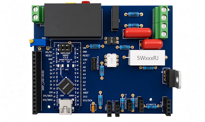
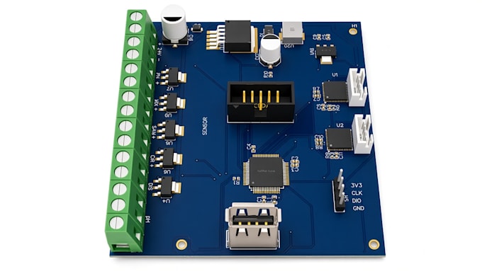
Hai bisogno di aiuto per ricreare un PCB esistente ma non hai i file di progetto originali? Posso reverse engineerare il tuo PCB da schede fisiche, foto, Gerber, layout esistenti o documentazione disponibile e ricreare il progetto per ulteriori modifiche o produzione.
COSA POSSO FARE:
CONSEGNE:
Schemi, sorgenti di PCB modificabili, BOM, Gerber, file di foratura e pick-and-place quando richiesto.
IDEALE PER:
PCB vecchi o danneggiati
Prodotti dismessi
File di origine mancanti
Duplicazione di PCB
Schede di ricambio
Prototipi e produzione
PERCHÉ SCEGLIERE ME:
Traccio attentamente le connessioni, organizzo i componenti e ricreo la scheda con una disposizione pratica e routing pulito.
SOFTWARE: KiCad | Altium Designer | EasyEDA
Hai un PCB, una foto, un Gerber o un progetto di riferimento? Inviamelo per una revisione prima di ordinare
Formato di file:
Gerber
•
STEP
•
3DS
•
Software:
Altium Designer
•
EasyEDA
•
KiCad
•
Matlab
•
Proteus
•
arduino
Interfaccia:
I2S
•
UART
•
USB
•
SPI
•
I2C
•
Wi-Fi
•
BLE
•
BT
•
GSM/GPRS
•
LTE
Traduzione automatica.
Puoi reverse engineerare un PCB fisico?
Sì. Invia foto chiare, misure e informazioni disponibili. Per schede più complesse, potrebbe essere necessario il PCB fisico.
Ho perso i file di progetto originali del mio PCB. Puoi ricrearli?
Sì. Posso ricreare lo schema e il layout di PCB modificabile dalla scheda e dalla documentazione disponibili.
Puoi ricreare un PCB dalle foto?
Sì, le foto possono essere usate per una prima valutazione. Immagini chiare di entrambi i lati, marcature dei componenti e dimensioni della scheda sono utili.
Puoi creare lo schema da un PCB esistente?
Sì. Posso tracciare le connessioni della scheda e ricreare lo schema basandomi sulle informazioni disponibili.
Puoi fare reverse engineering di PCB multistrato?
Sì, a seconda della struttura della scheda e delle informazioni disponibili. Le schede multilayer richiedono un'ispezione più dettagliata e potrebbero aver bisogno di informazioni aggiuntive.