Alcune informazioni sono riportate in lingua inglese.
Chi sono
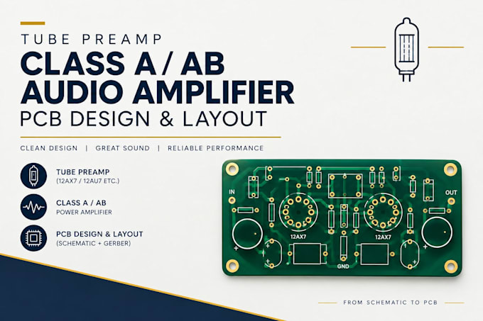
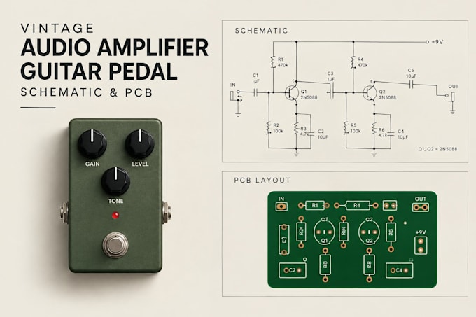
I am an electronics engineer specializing in schematic capture and professional PCB design. I help inventors, businesses, and electronics hobbyists turn circuit concepts, block diagrams, or prototype schematics into production-ready PCBs. My design workflow focuses heavily on DFM rules, proper component placement, and signal integrity to ensure layouts are clean, optimized, and ready for trouble-free fabrication at any major fab house. I provide multi-layer routing, BOM management, smart grounding, and standard Gerber packages. Message me with your requirements to get started!... Continua a leggere