PCB Design,Electrical electronic engineer,embedded system expert
Regno Unito
Inglese, Francese
Alcune informazioni sono riportate in lingua inglese.
Chi sono
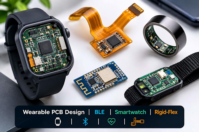
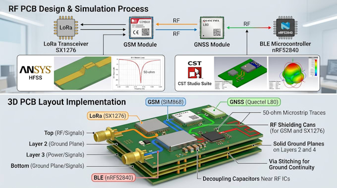
I am a professional PCB design engineer specializing in schematic design, multilayer PCB layout, RF circuit design, GNSS/GPS, BLE, and embedded hardware development. I deliver reliable, high-performance, and manufacturable designs tailored to your project requirements, from concept to prototype. My focus is on precision, quality, and practical engineering solutions that bring your ideas to life.... Continua a leggere