Sfoglia categorie
Esplora
Fiverr Pro
Italiano
$
USD

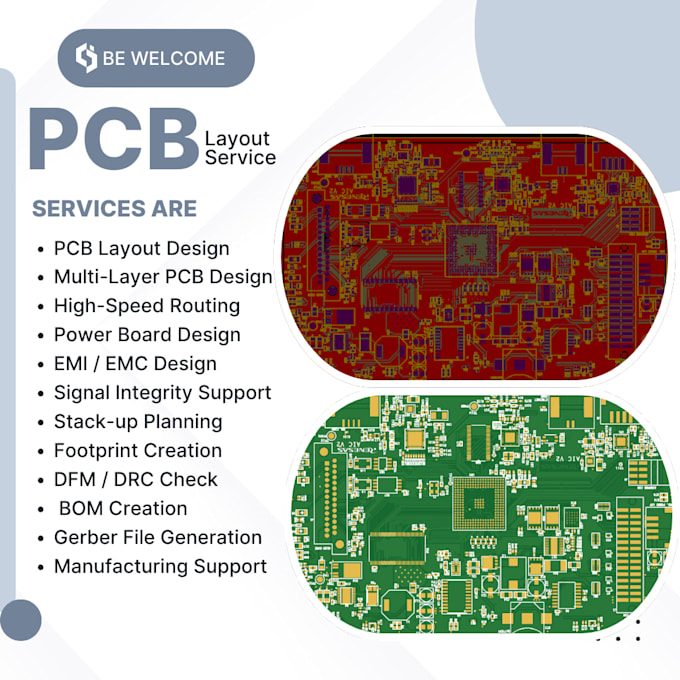
PCB LAYOUT DEIGNER
Competenze
Consulta i miei servizi
PCB Design Engineer
auklr technolys • Full time
Sep 2025 - Present • 8 mos
Developed PCBs for HMI clusters, telematics modules, IoT gateways, and EV control units. Executed impedance-controlled routing for MIPI-DSI, LVDS, USB, and Ethernet interfaces. Applied automotive EMC/EMI and reliability standards, improving product robustness. Designed compact, vibration-resistant layouts for two-wheelers, three-wheelers, and commercial EVs
