m
mihikansha

Mihikansha

@mihikansha

PCB Design Engineer, PCB Layout and Electronics Design

India
Inglese, Hindi
Alcune informazioni sono riportate in lingua inglese.
Chi sono
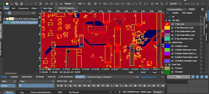
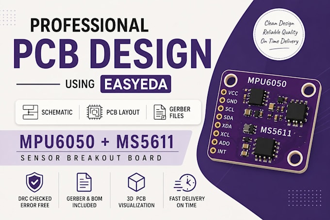
I specialize in PCB design using KiCad and EasyEDA. I can create schematics, PCB layouts, component placement, routing, and manufacturing-ready Gerber files. I focus on clean, reliable, and manufacturable PCB designs based on client requirements.... Continua a leggere

Competenze

m
mihikansha
Mihikansha
offline • 
Tempo di risposta medio: 1 ora

Consulta i miei servizi

Circuito stampato (PCB)
I will design pcb in kicad or easyeda

Esperienza lavorativa

Self_Employed

PCB Designer

Self Employed • Freelance

Aug 2026 - Present0 mos

I provide PCB design services using KiCad and EasyEDA, including schematic design, PCB layout, component placement, routing, design verification, and manufacturing-ready Gerber files. I focus on creating clean, reliable, and well-organized PCB designs based on client requirements.