Sfoglia categorie
Esplora
Fiverr Pro
Italiano
$
USD
Full Stack Software Engineer
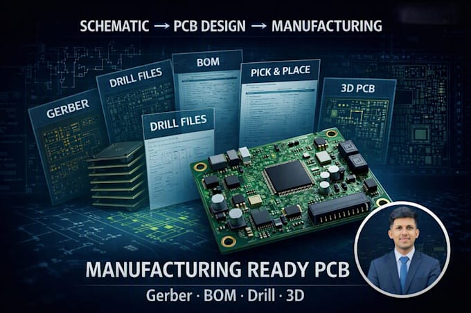
Need to turn your schematic into a professional PCB ready for manufacturing?
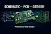
I will convert your electronic schematic into a clean and reliable PCB layout and provide the required Gerber and manufacturing files.
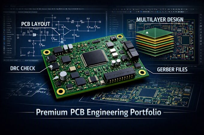
My service includes component placement, PCB routing, footprint assignment, board outline, copper zones, power and ground routing, design rule checking (DRC), and preparation of manufacturing files.
I can work with various electronic projects including STM32, ESP32, Arduino, sensor boards, IoT devices, control boards, power supplies, digital and analog circuits.
Depending on your package, I can provide:
Interfaces can include UART, USB, SPI, I2C, CAN, Ethernet, I2S, Wi-Fi, Bluetooth and other common interfaces.
Please provide your schematic, BOM/component list, PCB dimensions, required layer count and any manufacturer requirements.
Send me your schematic and let's turn your circuit into a professional PCB ready for manufacturing!
What files do you need to start the PCB design?
Please provide your schematic, BOM/component list, PCB dimensions if available, required number of layers, component datasheets for unusual parts, and any manufacturer or mechanical requirements.
Can you convert my schematic into a PCB layout?
Yes. I can convert your completed schematic into a PCB layout, assign footprints, place components, route connections, perform DRC, and prepare the required manufacturing files.
Will I receive Gerber files?
Yes. Gerber and drill files are included in the Standard and Premium packages. These files can be provided for PCB fabrication.
Can you create custom footprints?
Yes. I can create custom PCB footprints when a suitable standard footprint is not available. The number of custom footprints depends on your selected package.
Can you design multilayer PCBs?
Yes. I can work with multilayer PCB designs. The available layer count depends on the package you select and the complexity of the project.
Do you provide the source PCB files?
Yes. Source files are included according to the selected package, allowing you to continue editing the PCB design.
Can you provide BOM and Pick & Place files?
Yes. BOM and Pick & Place files can be provided with the applicable Standard or Premium package.
Can you work with complex or high-speed PCB designs?
Please contact me before ordering for complex, high-speed, RF, DDR, PCIe, controlled-impedance, or other advanced PCB projects so I can review the requirements and confirm the scope.