Sfoglia categorie
Esplora
Fiverr Pro
Italiano
$
USD
Design intelligenti, per soluzioni nel mondo reale
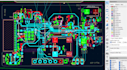
Progetterò il tuo schema di PCB per smartwatch industriale (ESP32 / sensori / display / alimentazione), BOM e indicazioni per il posizionamento in modo rapido e pronto alla produzione.
Cosa consegno (per servizio):
Pagine schematiche pulite di KiCad/EasyEDA (PMIC + batteria, MCU/modulo, sensori, display, pad di programmazione)
BOM compatto (CSV) prioritario per JLCPCB/LCSC con numeri di parte alternativi
Schizzo di posizionamento e keepout per PPG, antenna e finestra del display
Consigli su alimentazione e stackup (4-layer), guida DRC e note di assemblaggio
Perché scegliere me: Costruisco hardware IoT indossabile (tracker ESP32 e dispositivi smart home), ottimizzo per durata della batteria e facilità di produzione, e fornisco parti che JLCPCB/LCSC può reperire.
Come lavoriamo: Inviami le tue esigenze, il tempo di funzionamento desiderato (ore) e i componenti preferiti (o lasciami scegliere). Ti consegnerò uno schema professionale + BOM e ti guiderò nei prossimi passi verso il layout del PCB e la produzione.
Hai bisogno di firmware o di routing completo del PCB? Controlla i miei servizi extra o scrivimi, ti farò un preventivo personalizzato.


Formato di file:
Gerber
•
STEP
•
SCH
•
3DS
•
Software:
KiCad
•
LTspice
•
Matlab
•
NI Multisim
•
Proteus
•
Tina Ti
Interfaccia:
HDMI
•
I2S
•
UART
•
USB
•
SPI
•
I2C
•
SDIO
•
PCIe
•
Wi-Fi
•
BLE
•
BT
•
GSM/GPRS
Traduzione automatica.
Supporti la progettazione di PCB ad alta velocità?
Sì! KiCad 9 supporta il controllo dell'impedenza e la regolazione della lunghezza.
Quali produttori di PCB consigli?
JLCPCB, PCBWay o OSH Park a seconda delle tue esigenze.


