Sfoglia categorie
Esplora
Fiverr Pro
Italiano
$
USD
pcb deisgn and firmware development
Hello and Welcome!
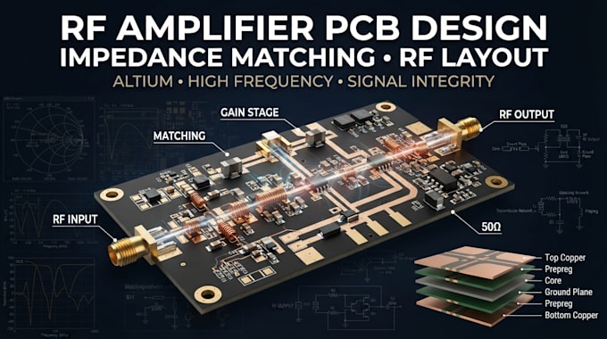
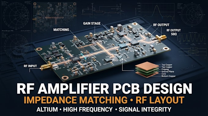
At RF frequencies, PCB geometry becomes part of the circuit. Trace width, dielectric height, return paths, grounding, component placement, parasitic effects, and impedance transitions can directly influence gain, stability, insertion loss, noise, and overall amplifier performance.
I will design your RF amplifier PCB with impedance matching, Altium and professional RF layout, focusing on controlled-impedance transmission lines, optimized RF signal paths, grounding, power distribution, and practical manufacturability.
WHAT I WILL PROVIDE:
WHY CHOOSE ME:
Message now and let get started!!!
Can you design RF amplifier PCBs?
Yes. I can design RF amplifier PCBs with optimized placement, RF routing, grounding, impedance control, matching networks, and manufacturing considerations.
Can you handle impedance matching?
Yes. I can implement impedance-matching networks and controlled-impedance transmission lines according to your RF specifications and PCB stackup.
Can you design 2GHz–2.4GHz RF PCBs?
Yes. I can handle RF PCB layouts for 2GHz–2.4GHz applications, including amplifier, wireless, and RF front-end circuits.
Can you design RF power amplifier boards?
Yes. I can handle the PCB implementation of RF power amplifier stages, including RF routing, grounding, power distribution, thermal considerations, and connector integration.
Can you work with high-frequency RF circuits?
Yes. I can design layouts involving high-frequency transmission lines, microstrip/stripline structures, RF connectors, matching networks, and controlled-impedance routing.