Sfoglia categorie
Italiano
$
USD
Connettiti alla tua IA
PCB Design KiCad, Altium, EasyEDA Gerber, BOM, CPL for JLCPCB
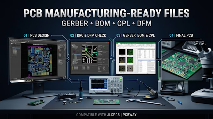
Your PCB gets delayed when the manufacturer rejects the files. I prepare manufacturing-ready PCB files for JLCPCB and PCBWay: Gerber, drill, BOM and CPL (pick and place), checked against the fab's capabilities before you order.
Pick what you need
Rejections I fix
Rotated parts in the CPL file, wrong footprints, missing LCSC numbers, stackup mismatch, drill and solder mask errors.
Delivery pack
Zipped Gerbers, drill files, BOM (CSV), CPL, PDF schematic, source project.
Already have a board? Message me the files and I will confirm the right package.
Will the files pass the JLCPCB and PCBWay upload check?
Yes. Every pack is DRC-checked and set to the manufacturer's limits for trace width, clearance, drill size and stackup before delivery.
What do I send for BOM and CPL files?
Your project file (KiCad, Altium, EasyEDA) or Gerbers plus a parts list. For assembly I match parts to LCSC numbers and correct rotation and polarity offsets.
Can you clone or reverse engineer an existing PCB?
A: Yes, from Gerbers, high-resolution scans or photos with measurements. You get an editable schematic and layout. Complex multilayer boards need a custom offer.
Can you fix errors in a board I already designed?
Yes. I review clearances, annular rings, silkscreen, footprints and polarity, correct them and send updated production files.
