Sfoglia categorie
Italiano
$
USD
Connettiti alla tua IA
Senior PCB Design Engineer, Altium, KiCad and Reverse Engineering
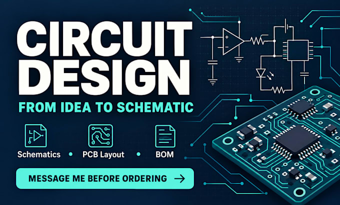
Need reliable electronic circuit design and production-ready multilayer PCB layout? As a Senior Hardware & PCB Design Engineer with 6+ years of experience, I turn your concept or block diagram into first-pass working hardware in Altium Designer, KiCad, or EasyEDA.
What I Design:
- Embedded & IoT: ESP32, STM32, Arduino, nRF, RP2040
- Power Electronics: DC-DC Buck/Boost, LDO, Li-ion BMS, Motor Drivers
- Industrial & High-Speed: 2-to-8 Layer PCBs, RS-485, CAN, Ethernet, USB-C, Sub-GHz RF
- Analog & Sensor Conditioning: Op-amps, ADC/DAC, isolation & EMI/ESD protection
Turnkey Deliverables (JLCPCB, PCBWay & EU Fabs Ready):
- Editable Schematics & PCB Source Files
- RS-274X Gerbers & NC Drill Files
- Calibrated Pick & Place (CPL) & LCSC/Digi-Key BOM
- 3D STEP Mechanical Models & Schematic PDFs
- 100% ERC/DRC Verified with DFM/DFA Checks
Message me before ordering with your block diagram, specs, or constraints so we select the right package!
Can you design a circuit from an idea without an existing schematic?
Yes. Describe what the circuit should do, the supply voltage, inputs and outputs, and any size or component limits. We will agree on the requirements and deliverables before you place an order.
What files will I receive for manufacturing and SMT assembly?
You receive native Altium, KiCad, or EasyEDA source files, RS-274X Gerbers, NC Drill, PDF schematics, 3D STEP models (Standard/Premium), a sourced LCSC/Digi-Key BOM, and a calibrated Pick & Place (CPL) file ready for JLCPCB, PCBWay, or any fab.
Which EDA software tools do you use?
I work natively in Altium Designer, KiCad, and EasyEDA, and can match your preferred toolchain or company design standards.
Do you design 4-layer, 6-layer, and high-speed PCBs?
Yes. I design 2-to-8 layer PCBs with controlled impedance, dedicated ground/power planes, differential pair routing (USB, Ethernet, CAN), and EMI/ESD protection.
Are your designs ready for JLCPCB or PCBWay SMT assembly?
Yes. Every design undergoes strict ERC/DRC and DFM/DFA verification, using parts with verified footprints, active stock, and calibrated CPL orientation for turnkey SMT assembly.
What should I send before placing an order?
Please share your project goals, supply voltage, key interfaces or sensors, board size constraints, and any reference schematics or datasheets so we can select the best package.
