Sfoglia categorie
Esplora
Fiverr Pro
Italiano
$
USD
PCB DESIGN AND FIRMWARE DEVELOPMENT
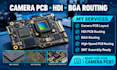
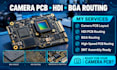
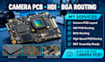
A great camera board is not just about connecting componentsits about getting high-speed signals, tight BGA escape routing, HDI structures, and manufacturing constraints to work together without creating expensive surprises later.
What You Will Get
What Makes Me Stand Out
I focus on the problems that can appear after fabricationnot simply making traces connect. I consider signal integrity, spacing, manufacturability, thermal paths, and assembly requirements throughout the layout process.
Deliverables
Gerber files, drill files, BOM/position files where required, source PCB files, and manufacturing-ready outputs.
Have a challenging camera PCB? Send your schematic and requirements, and lets turn them into a board ready for the next stage.
Can you handle BGA routing on camera PCBs?
Yes. I can handle BGA fanout and routing while considering layer count, spacing, via structures, and manufacturing constraints.
Can you work with HDI PCB requirements?
Yes. I can work with HDI structures such as microvias, via-in-pad, and high-density component routing based on your manufacturer’s capabilities.
Can you route high-speed camera interfaces?
Yes. I can route interfaces such as MIPI CSI-2 and other high-speed connections according to the provided specifications and stackup requirements.
Will the PCB files be ready for SMT manufacturing?
Yes. I can prepare manufacturing and assembly outputs such as Gerbers, drill files, BOM, and pick-and-place files when required.
What do you need to start the project?
Please provide your schematic, component/BOM files, board dimensions, stackup requirements, manufacturer capabilities, and any specific routing constraints.


