Sfoglia categorie
Esplora
Fiverr Pro
Italiano
$
USD
PCB Design Reviewer Schematic Specialist
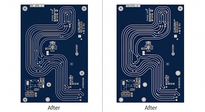
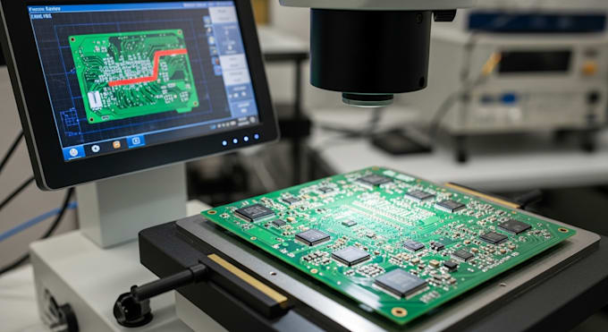
Getting a PCB back from the factory only to find a silly footprint error or a noisy power rail is the worst feeling. Most design fails happen because of small oversights that EDA tools just don't catch. I look at your boards through the lens of a manufacturer to make sure they actually work when they arrive.
I don't just run a DRC and call it a day. I dig into your component selection, signal integrity, and thermal management. If your high-speed traces are too close or your decoupling caps are poorly placed, I will find it before you spend money on a bad prototype.
Service Included:
- Footprint accuracy verification
- Schematic logic and netlist check
- Signal integrity and EMI analysis
- DFM analysis for easy assembly
- Thermal relief and copper pour review
- Bill of Materials (BOM) optimization
- Gerber file validation
How it works:
1. You send your design files and requirements
2. I perform a deep-dive manual review
3. You get a detailed report with fixes
Send over your project files and let's make sure this board is solid.


Which software tools do you support?
A: I am most comfortable with Altium Designer, KiCad, and Eagle, but I can review PDF schematics and Gerber files from any tool.
Do you fix the errors or just list them?
The Standard and Premium packages include a report and direct implementation of minor fixes if you provide the source files. Major architecture changes require a custom quote.